How Semiconductor Process Technology Affects ASIC Miner Profitability
Just because a miner is an ASIC Miner does not mean that it is automatically the most profitable device available. Application-specific integrated circuits are made with a specific process technology, and the process technology is usually referred to by the smallest feature size of any of the transistors on the integrated circuit.
One of the problems with bringing ASIC miners to the market is that they could put such a large hashrate on to the network, that for most people it is uneconomical to run the miner. The amount of electricity used would be significantly more than the amount of coin mined.

Cryptocurrency mining is an industry which tends to balance out with people that are operating the miners in a low cost electricity and business operating environment. These businesses will continue operating them, and the ones that operate in a less profitable environment will shut them off and possibly sell them.
So for example, the antminer D3 is, I believe, a 28 nm process technology for the X11 algorithm used to mine Dash. Unfortunately the first is that these machines were brought out when the overall crypto market prices were going down, they were much more efficient compared to GPU miners or the previous generations of ASIC Miners, and they were produced in unexpectedly large volumes. Given all that, for most people the antminer D3 was an unprofitable device after the first few months of running it.
In the time since that antminer D3 was brought to Market, other manufacturers brought to Market much more efficient X11 Asic miners. These miners are on the order of 10 to 12 times more power efficient than the D3. Anybody that wants to mine Dash, would buy one of these new miners.
As the feature size get smaller, the upfront expenses to design and do a test run of the semiconductor gets more expensive. In the last few years, what we see most commonly come out in the first version of a purpose-built Asic Miner for an algorithm is typically done on a 28-nanometer process technology.
The size of the die for each integrated circuit as well as the number of transistors is roughly proportional to the amount of energy used and heat produced. And from a rough standpoint, the feature size can be squared in order to compare it’s energy use to the other features sizes
| Feature Size | Squared | Notional Hashrate at 1000W | Efficiency compared to 28 nm miner |
| 28 nm | 784 | 1,000 | 1 |
| 16 nm | 256 | 3,062 | 3.1 |
| 10 nm | 100 | 7,840 | 7.8 |
| 7 nm | 49 | 16,000 | 16 |
On a relative basis a 16 nm chip will be 3 times as energy efficient as a 28 nm chip. A 10 nm chip will be 8 times as efficient, and a 7 nm 16 times.

This works for other ratios as well. Theoretically, an efficient 7 nm Bitcoin miner should be about 16/3.1, or 5 times as power efficient as a 16 nm Bitcoin miners.
It’s not that simple, of course, but these rough calculations are a good guide to relative potential efficiency. These rough power assumptions are relative and assume that everything else about the design stays the same. There are some extremely talented ASIC designers that are able to make their designs much more efficient, and even more important, make them in such a way that the end result tests out well and operates reliably in production.
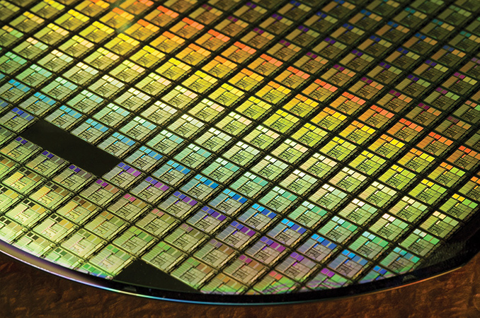
When a semiconductor wafer is produced with many small integrated circuits on it, each of these IC’s needs to be tested. Some test and fail, others test and are mediocre in their performance, and others test in are outstanding in their performance. The difference depends on the amount of impurities that are in the semiconductor wafer when it’s created. This testing process is sometimes called binning. This is the semiconductor wafer yield, and it determines how profitable a given semiconductor wafer run is.
It’s relatively straightforward to come to market with a 28 nm design, because the upfront expenses are not that much, it can be brought to market quickly, are the features are relatively big so that errors don’t affect the chips as much. It makes for a good first cut of an ASIC Miner.
The latest technology that’s used for large amounts of semiconductors is the 7 nm process. When a new process technology is ramped-up into production, the people who need it the most, which is usually the cell phone and memory manufacturers, are willing to pay for wafer for availability.
There is a limited amount of availability because an entire new wafer manufacturing facility needs to be built for each new generation, with all the equipment replaced. It is a multibillion dollar investment to build a state of the art new generation wafer fab.
When a wafer run is made, thousands of chips are produced, and then it’s up to the manufacturer to sell them profitably.
Having said all that, if Bitcoin and Litecoin mining Asics start being produced in volume at 7 or 10 nm with a good design that gets good yield, those will be worth buying, because they will have a potential lifetime of two to four years at decent profitability.


